413 Series
Substrate and tape total and individual thicknesses, warpage, and TTV Measurement. Able to measure with or without backing tape. For wafer back-grind and etch thinning processes control. Non-contact Echoprobe or VITE Technology. Thin film and surface roughness options.
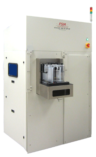
413 C2C
Thickness and total thickness variation (TTV) mapping system. TTV and Thickness of wafer substrate, thick layers, wafers on tape, bonded wafers, etc. Fully automated cassette to cassette system, SECS/GEM compliant. Warp, Roughness, and Thin Film Thickness measurement options.
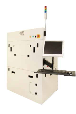
413 SA
Thickness and total thickness variation (TTV) mapping system. TTV and Thickness of wafer substrate, thick layers, wafers on tape, bonded wafers, etc. Semi-automatic system with enclosure. Manual loading, automatic measurement. Warp, Roughness, and Thin Film Thickness measurement options. Systems up to 300mm diameter wafers with or without frame.
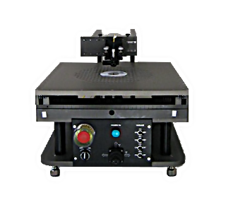
413MOT
Thickness and total thickness variation (TTV) mapping system. TTV and Thickness of wafer substrate, thick layers, wafers on tape, bonded wafers, etc. Manual loading, auto-mapping. Warp, Roughness, and Thin Film Thickness measurement options. Systems up to 300mm diameter wafers with or without frame.