128 Series
Frontier Semiconductor is the leading manufacturer of stress measurement tools for semiconductor, MEMS, optoelectronic, and flat panel applications. Stress and wafer bow maps can be acquired over the entire wafer surface, providing process engineers means to characterize and develop new processes using different thin film materials.
The FSM 128 Series systems are room temperature, full-wafer 2D/3D stress mapping systems. 128 systems use FSM's patented non-contact Opti-Lever dual-laser auto-switching technology featuring a micropositioning detector to measure the laser beam deflection with high precision over a large dynamic range of small to large bow or stress. FSM's stress gauges have the ability to scan 1000 points per inch in seconds for high resolution, high precision stress mapping on blanked and patterned wafers.
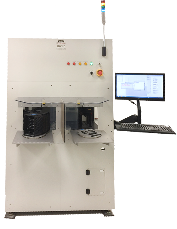
128 C2C
Dedicated Film Stress mapping system with high resolution for high throughput process control for wafers up to 200mm diameter. Fully automated cassette to cassette, SECS/GEM Film Stress and Bow Measurement tool. Dual or single load port configurations available. Integrated wafer substrate thickness measurement available.