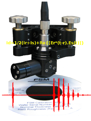
Thin wafer metrology
Thinning and backgrinding of wafers requires precise control of thickness, total thickness variation (TTV) and warp. FSM offers solutions for measurement of wafers and wafers on tape.
413 Series
Substrate Thickness, Warp, and TTV Measurement
with or without Tape
for Wafer Backgrind and Etch Thinning processes.
Non-contact Echoprobe Technology.
Thin film and surface roughness options.
413 C2C 413 SA 413MOT
413 C2C 413 SA 413MOT