Film Stress
Film stress and and wafer bow measurements are an integral part in the process of reliability monitoring of deposited thin films during the chip making process.
Stress monitoring has become increasingly critical with the advent of 3D integrated circuits.
There are three types of film stress: global, local, and lattice level stress. FSM offers solutions for all three types in our 128/500/900 Series, 127 Series, and Raman 360 tools.
128 Series
500 Series
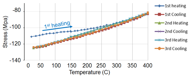
Stress Hysteresis Measurement up to 500C for thermal property and stability tests of thin films in air.
500TC
900 Series
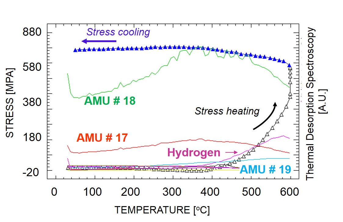
Stress Hysteresis in vacuum or gas up to 900C for the study of annealing cycles. Thermal Desorption, Film Shrinkage, Reflectivity, and Resistivity options provide additional insight to causes of material changes with temperature.
900 C2C 900TC-VAC