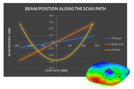
Laser Scanning
FSM uses patented Laser Scanning technology to measure the radius of curvature and bow of wafers. A laser beam is directed to the wafer. The beam is reflected at an angle that corresponds to the radius of curvature of the wafer.
128 Series
Bow and Global Film Stress Measurement.
Non-contact full wafer stress mapping for semiconductor and flat panel application.
Dual Laser Switching Technology.
128L C2C 128L 128NT 128G-450 128 C2C 128 FPD
128L C2C 128L 128NT 128G-450 128 C2C 128 FPD
500 Series
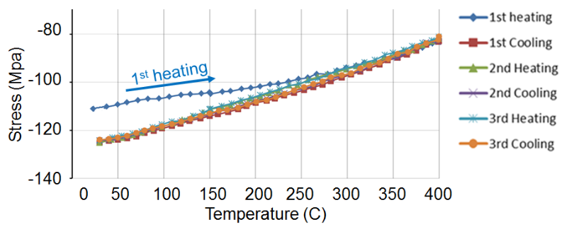
Stress Hysteresis Measurement up to 500C for thermal property and stability tests of thin films in air.
Non-Contact Laser Scanning Technology.
500TC
500TC
900 Series
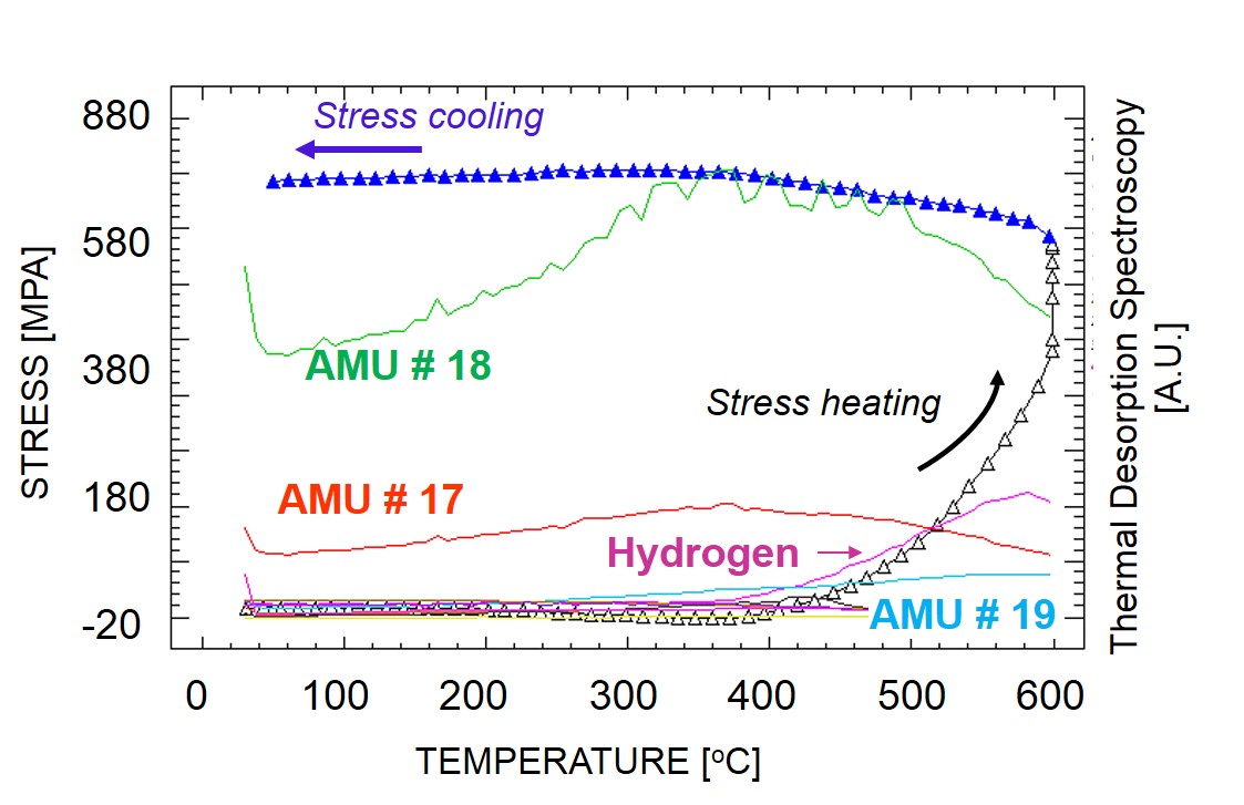
Stress Hysteresis in vacuum or gas up to 900C for the study of annealing cycles.
Thermal Desorption, Film Shrinkage, Reflectivity, and Resistivity options provide additional insight to causes of material changes with temperature.
900 C2C 900TC-VAC
900 C2C 900TC-VAC